The System Architecture of NES
In this blog, I will take a closer look at the NES, one of the most iconic gaming consoles to ever release and explore how its hardware worked.
In this blog, I will take a closer look at the NES, one of the most iconic gaming consoles to ever release and explore how its hardware worked. This blog is inspired by NesHacker and the video NES Architecture Explained. Please consider supporting their youtube channel since they’re providing some really useful information about the NES.
Introduction
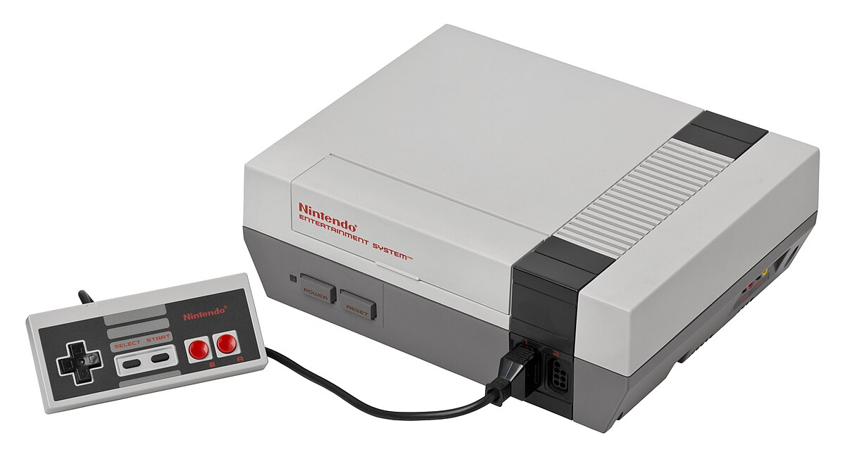
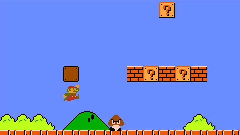
The NES is hands down one of the most iconic gaming consoles of all time. First released in Japan as the Famicom on July 15, 1983, the console would make its way to the US, being redesigned and named the NES, which stands for Nintendo Entertainment System, in 1986. Several games released on the NES, including Super Mario Bros. (1985), The Legend of Zelda (1986), Metroid (1986), Mega Man (1987), and EarthBound Beginnings (1989), went on to become worldwide favorites, strengthening the NES's position in console gaming. For this blog, I’ll take you through the NES’s architecture and explain how each component would communicate with each other to form a fully functioning game.
Overview
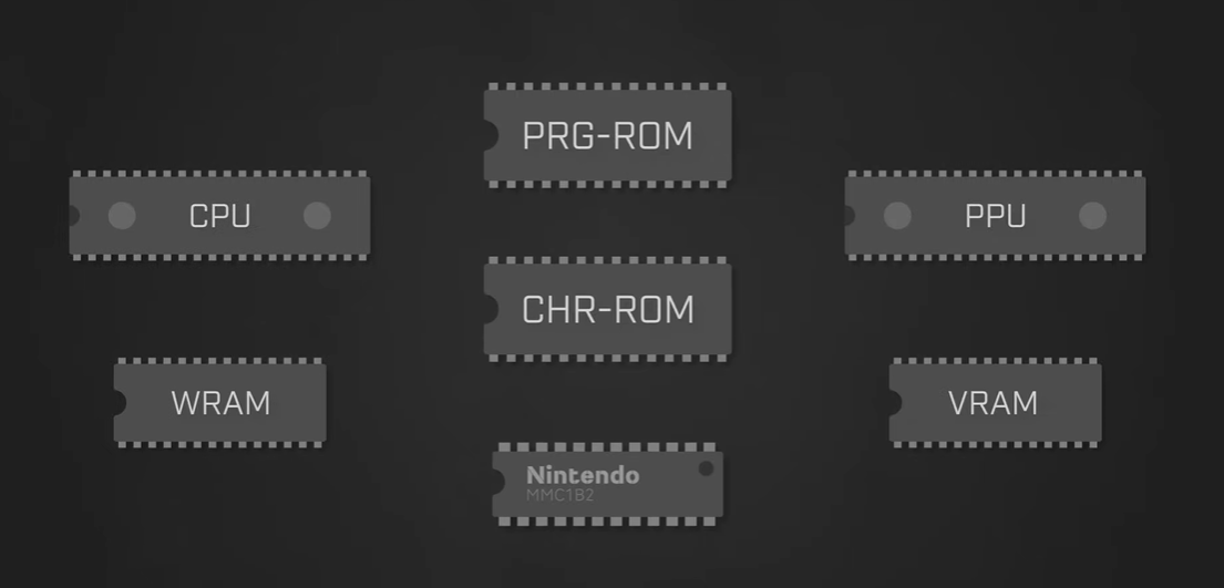
The NES’s major components can be broken down into three major groups: CPU-related, PPU-related, and cartridge-related components. The CPU and PPU components exist directly on the NES motherboard, while the cartridge components exist on each game cartridge and interface to the motherboard via the cartridge connector.
The Main Components
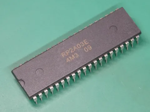
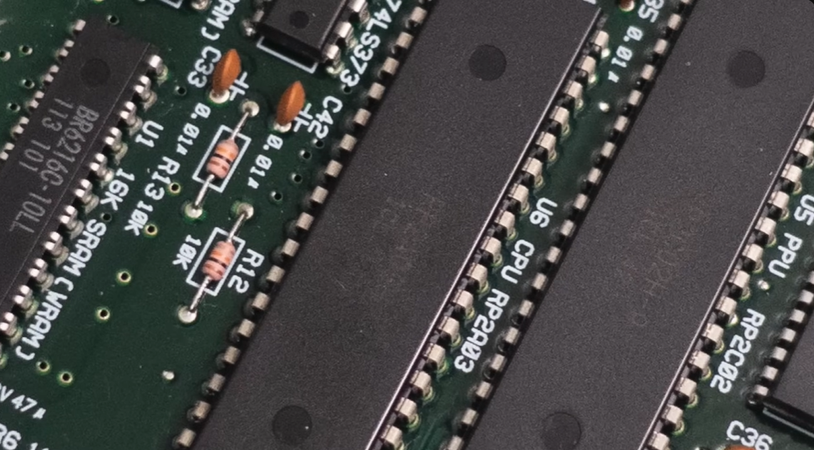
The first main components is the Central Processing Unit, which is a custom processor based on the MOS 6502.
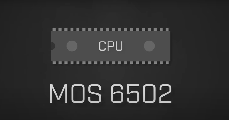
The CPU plays the role of being the main coordinator of the system and is largely responsible for telling basically every other component what to do. It’s the only part of the system that you have direct control over. So, when you write 6502 codes and assemble your games, this is what executes all the resulting machine codes.
The chip, which is RP2A03H for the NTSC system and RP2A07 for PAL, contains 2 processors: a modified 6502 lacking the decimal mode circuitry (more specifically, binary-coded decimal mode) and a custom audio processing unit, or APU for short. (fun fact: the chip was also used as a sound chip and secondary CPU by Nintendo's arcade games Punch-Out!! and Donkey Kong 3).
For now, you might already have 2 questions in your mind. “Why do Nintendo use that specific modified 6502 processor?” and “Why do they even use two different chips in the first place?”. What? You don’t have any questions about that at all? Well, I’m just going to answer them anyway.
Why Use That Specific modified 6502 processor? Nintendo chose the 6502 as their base processor for several practical reasons. First, it was significantly cheaper than competitors like the Intel 8086 or Motorola 68000, which was crucial for keeping console costs low. The 6502 was also simpler and more power-efficient, important factors for a home console that needed to be reliable and affordable. By the early 1980s, the 6502 had proven itself in successful computers like the Apple II and Commodore 64, so developers were already familiar with programming it. Nintendo's modification removed the decimal mode (BCD) circuitry that wasn't needed for gaming applications, freeing up chip space and reducing costs. They also integrated their custom Audio Processing Unit (APU) directly onto the same chip, creating an efficient single-package solution. This approach gave Nintendo a cost-effective, proven processor that could handle gaming tasks while keeping the overall system simple and affordable to manufacture.
Why Use Two Different Chips? The reason Nintendo used different CPU chips for different regions comes down to incompatible television broadcasting standards. NTSC (used in North America and Japan) operates at 29.97 frames per second with 525 scan lines, while PAL (used in Europe and Australia) runs at 25 frames per second with 625 scan lines. These aren't just simple display differences but the entire system timing had to match each television standard. The RP2A03 runs at approximately 1.79 MHz to sync with 60Hz NTSC displays, while the RP2A07 operates at 1.66 MHz for 50Hz PAL displays. This timing difference affects everything from game speed to audio pitch, which is why many PAL games run about 17% slower and have deeper-sounding music compared to their NTSC counterparts. Nintendo couldn't simply use the same chip for both regions because the CPU, PPU, and APU all needed coordinated timing to work properly with their respective television standards.
Oh, there’s also this fun additional information that I found online. You do rememeber earlier when I said that this processor lack the decimal mode circuitry right? Well, this chip was actually manufactured by a company called Ricoh (that why they’re usually called the Ricoh 2A03), and it contains an unlicensed derivative of the MOS Technology 6502 core. This Ricoh 2A03 is actually modified to disable the binary-coded decimal mode, which is possibly to avoid a MOS Technology patent.
CPU System Memory
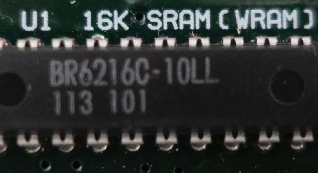
The next major component is the CPU system memory, which is represented by a single 2-kilobyte SRAM chip on the NES motherboard. This chip stores all the mutable data for a game. Things like animation timers, player health, score counters, and other variables that change during gameplay. This represents the primary memory that programmers work with when writing a game's algorithms and logic.
Picture Processing Unit (PPU)
Moving to the graphics side, we have the Picture Processing Unit (PPU) and its associated 2-kilobyte SRAM. The PPU is responsible for rendering a game's graphics and has a fixed set of functionality that cannot be programmed directly. Instead, rendering can be modified through memory-mapped input/output registers that can be manipulated by the CPU.
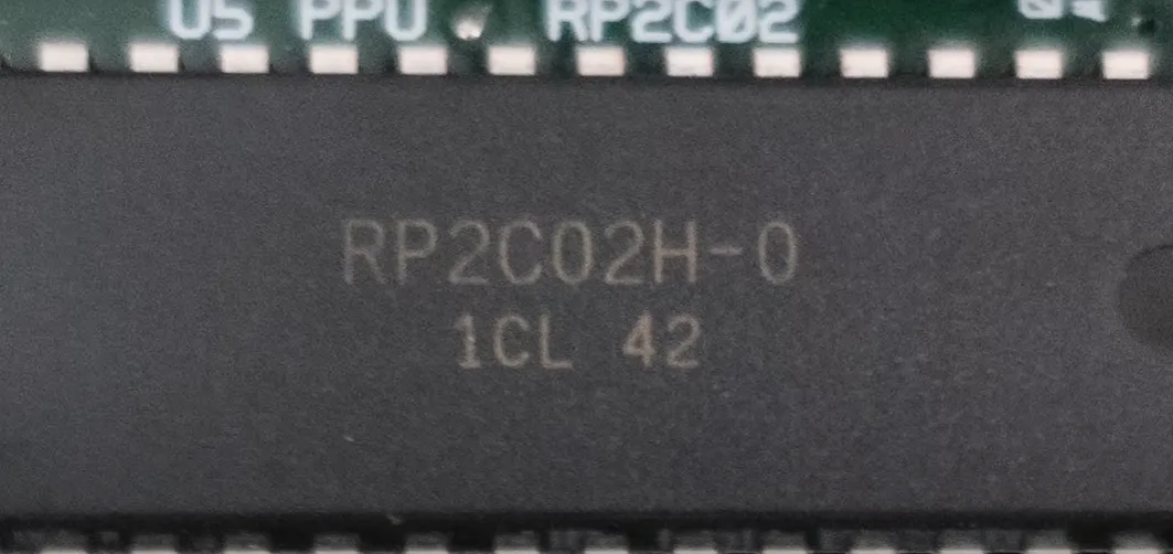
The PPU's SRAM, often called Video RAM or VRAM, is generally used to hold the name tables (which define what tiles appear where on screen), attribute tables (which control color palettes), and the palettes themselves. Additionally, it's used by the cartridge to control how a game mirrors name tables when performing screen scrolling effects.
Cartridge Components
The final group of components exists on the game cartridges themselves and provides game-specific information. Every cartridge contains several key components:
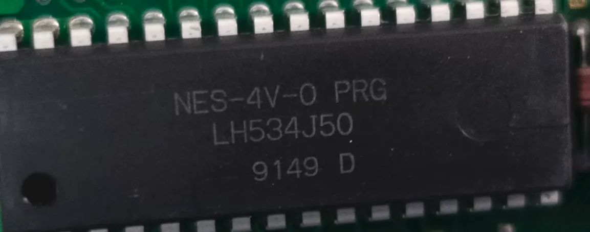
Program ROM: This chip stores the machine code for the game, all the set of instructions that tell the CPU what to do during gameplay.
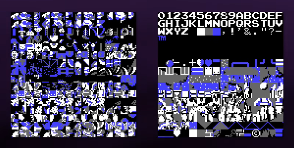
Character ROM/RAM: This chip stores the tile data, which consists of tiny 8x8 pixel images that are used to compose both the background and foreground graphics you see on screen.
Cartridge RAM: Some cartridges include their own general-purpose RAM chips that can be accessed directly by the CPU. In some cases, this RAM is kept powered continuously by a small battery soldered onto the cartridge's PCB, allowing for the storage and retrieval of save game information.
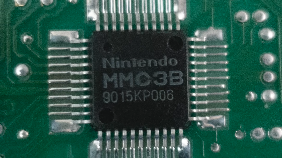
Memory Mappers: Many games also contain special chips known as mappers, which can change the behavior or output of other chips on the cartridge. Programs generally control a mapper by writing data to specific memory-mapped I/O locations dictated by the hardware on the cartridge itself.
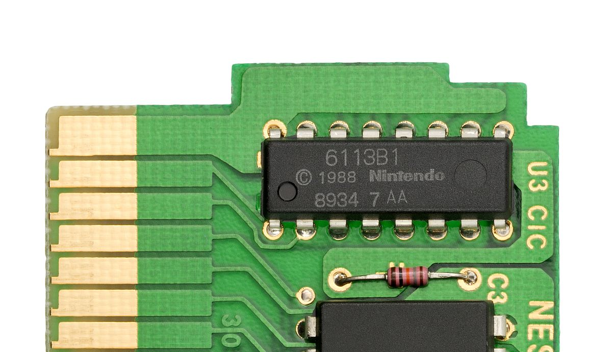
Another components that you would usually find on a cartridge is the CIC Lockout chip, but when it comes to the overall system architecture, it does not really play a big role.
So that’s basically all the main components of the NES. Next, we would have to know how everything communicate with each other in order to run a game.
Digital Circuits: The Foundation
Before diving into how NES components communicate, it's helpful to understand the basics of digital circuits. At their core, digital circuits consist of only two basic ingredients: components and wires that connect those components.
Think of the wires as highways down which information travels, while the components are like factories that process that information. In the NES, these "factories" include the CPU, PPU, RAM chips, and ROM chips, each performing specific tasks with the data they receive.
Digital Signaling: Speaking in Binary
Digital circuits use a special type of signaling based on voltage levels to communicate binary information. The NES uses a common scheme where low voltages represent zeros (0) and high voltages represent ones (1)
This means any given wire or trace on the NES's printed circuit board can hold exactly one bit of information at a time—either a 0 if it's at low voltage or a 1 if it's at high voltage.
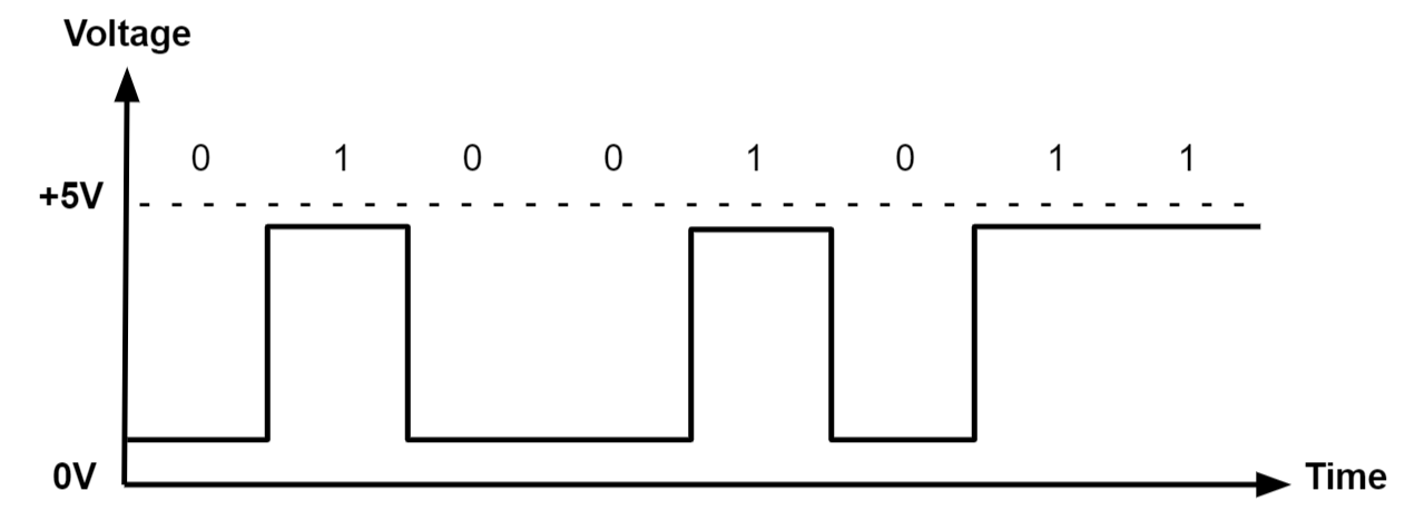
Taking this concept further, any component on the board can only handle an amount of data equal to the number of data wires connected to it. If a component has 8 data wires connected, it can process 8 bits (1 byte) of information simultaneously.
But it's worth noting that not all wires on the circuit board carry data. Some provide electrical power to keep components running, while others carry analog signals like the RF output that gets sent to your television. But when they do carry data, these wires are typically organized into groups for efficiency and clarity.
How Components Communicate: The Bus System
Understanding how these components talk to each other requires grasping the concept of buses. In digital circuits, components are connected by wires that carry information, and these wires are often grouped together into something called a bus.
As mentioned above, the NES uses digital signaling where low voltages represent zeros and high voltages represent ones. Any given wire can hold exactly one bit of information at a time, so components can only handle an amount of data equal to the number of wires they're connected to.
The Main System Buses
An 8-bit computer like the NES generally has two major buses:
Data Bus: Contains eight wires and is used to communicate byte-sized information between components.
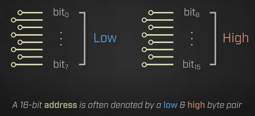
Address Bus: Usually 16 bits in length and is used to communicate memory addresses—essentially telling the system which piece of data to access.
Every component that needs to access or manipulate data must be connected to both of these buses. The address bus tells the system which data to access, while the data bus provides the actual binary information.
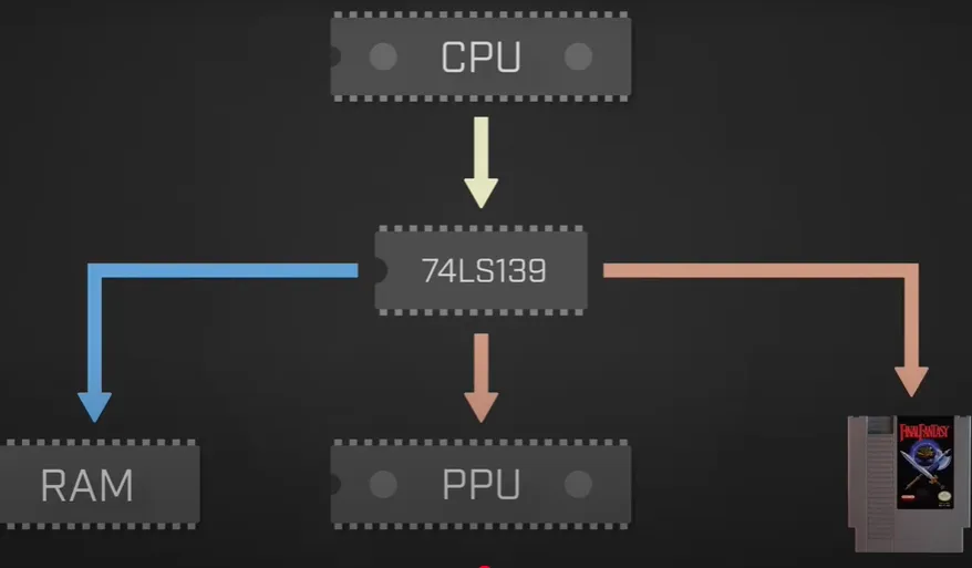
Memory-Mapped I/O: The Traffic Control System
With everything connected to the same buses (which is the fundemental organizing principle underlying the majority of every modern computers), you might wonder how components know when they're supposed to send or receive data. The answer lies in a technique called memory-mapped I/O.
Memory-mapped I/O segments the system's overall memory space into multiple regions and assigns each region to a specific piece of hardware. For the CPU memory space, this creates four main segments: System RAM (first segment), PPU I/O registers (second segment), APU registers (third segment) and Cartridge space (final segment)
Each hardware component has a special "chip select" or "chip enable" pin that works like an on/off switch. When this pin receives a low voltage (0), the chip turns on and can send or receive information via the data and address buses. When it receives a high voltage (1), the chip turns off and ignores the buses.
How Memory Access Works
To learn how memoru access works on the NES, we can trace through a typical memory access operation below:
- The CPU places an address on the address bus
- Special discrete logic chips on the motherboard decode this address
- Based on the address, these chips generate appropriate chip select signals
- Only the component responsible for that memory region gets activated
- The activated component either provides data to the CPU or receives data from it
For example, if the CPU wants to read from address $0305 (which corresponds to system RAM), the discrete logic hardware determines this belongs to RAM, turns off the cartridge and PPU, and turns on the system RAM chip. The RAM then provides the requested data on the data bus.
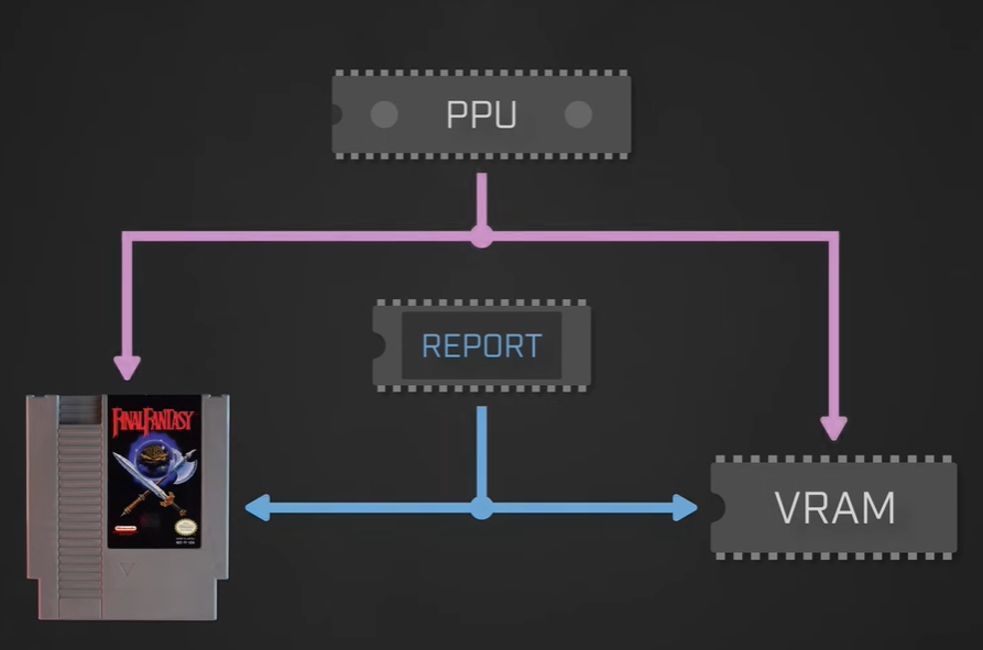
The PPU's Separate World
The PPU operates somewhat differently from the CPU side of things. It has two main responsibilities:
Respond to CPU requests: The PPU must react to the CPU via chip select signals and the main system buses, either providing information back to the CPU or processing information given to it.
Render graphics: The PPU must actually draw the game's graphics by leveraging information from its internal registers along with data from VRAM and the cartridge.
PPU Bus Architecture
To communicate with VRAM and the cartridge, the PPU uses a single hybrid bus that handles both addresses and data. This bus is split into two parts:
Lower 8 bits: Represent both data and the first 8 bits of addresses
Upper 6 bits: Represent the rest of the address
The PPU uses a clever technique with a digital latch to manage this shared bus. First, it outputs the address it wants to access, triggers the latch to remember the address, then switches the lower 8 lines to handle data transfer.
Cartridge Architecture: The Game's Hardware Brain
Cartridges are more than just storage devices—they're essentially expansion modules that can significantly alter how the NES behaves. The cartridge's PCB connects its chips to the system through the cartridge connector's pins.
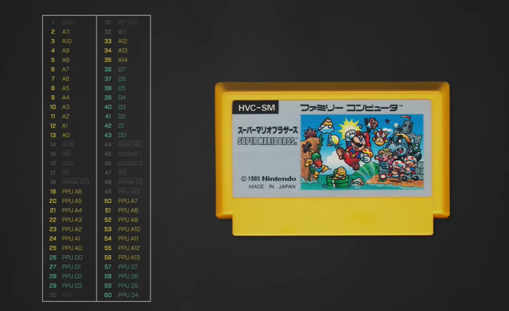
Pin Layout
Looking at a Famicom cartridge (which is functionally equivalent to NES cartridges but simpler to analyze), we see:
- 60 total pins
- 4 pins for electrical power
- 45 pins dedicated to address and data buses
- Remaining pins for control signals
Interestingly, the NES doesn't provide the full 16-bit CPU address to cartridges. Since program ROM only occupies the upper half of the CPU's memory space, it only needs 15 bits. For character ROM, the system provides 14 bits, allowing for 8KB of character data plus potential cartridge VRAM.
Memory Mappers: Breaking the Limits
One of the most ingenious aspects of NES cartridges is the memory mapper system. The NES's 16-bit address space imposes strict limits on how much data can be accessed at once, but mappers allow games to exceed these constraints.
Mappers split ROM and RAM chips into banks that can be swapped in and out as needed. When a game's program writes data to specific program ROM addresses, the mapper interprets this as a control message and changes its behavior—perhaps swapping to a different bank of graphics data or program code.
Different mappers (like the famous MMC3) can also provide some more advanced features, such as:
- IRQ interrupts: Sending signals to halt CPU execution at specific moments
- Advanced graphics techniques: Allowing palette changes mid-frame
- Bank switching: Dynamically loading different code and graphics
Cartridge RAM
Many cartridges include additional RAM chips, typically occupying memory addresses starting around address $6000 and ranging from 2 to 8 kilobytes in size. These chips supplement the system's built-in RAM and are coordinated by the mapper chip based on addresses provided by the CPU.
Putting It All Together
The NES architecture is elegant in its simplicity while also being quite sophisticated in its execution. The system leverages centralized buses with memory-mapped I/O to coordinate between CPU, PPU, and cartridge components. Discrete logic chips decode addresses to enable and disable components on shared buses, while the PPU maintains its own specialized bus for graphics operations.
Cartridges extend this architecture through their own internal bus systems, connecting ROM and RAM chips to the main system while using memory mappers to break through the limitations of the 16-bit address space.
This architectural approach has allowed Nintendo to create a system that was both affordable to manufacture and flexible enough to support increasingly complex games throughout its lifespan. From simple early titles to advanced later games that pushed the hardware to its limits, the NES architecture proved remarkably adaptable.
Understanding this architecture provides us with crucial insight into how 8-bit games were designed and why certain programming techniques were necessary. It's a testament to thoughtful engineering that created one of gaming's most enduring platforms.
Conclusion
The NES architecture represents what we could call a masterclass in balanced design, powerful enough to create memorable gaming experiences while simple enough to be affordable and reliable. By understanding how these components work together, we can gain appreciation not just for the technical achievements of the era, but for the creativity of developers who worked within these constraints to create gaming's most beloved classics.
Whether you're interested in retro gaming, computer architecture, or just want to understand how one of gaming's most important systems worked, the NES provides a fascinating case study in effective hardware design that continues to influence gaming systems today.
Read more at: Lazzerex’s Blog
Source: Published Notion page
This article
Post Reactions
Join the conversation
Write a Comment
Share your thought about this article.
Comments
Loading comments...